
Submitted by ok1rr on
Many years ago I wanted to test RTTY and the new digital modes. Not too seriously, with a simple interface in KISS (Keep It Simple Stupid) style. There is nothing to improve, except my awful PCB design matched to the box I discovered in my junk store.
For AF isolation I used small transformers made by Neutrik AG of unknown type with 1kohm/1kohm ratio with wire leads. For the keying circuit, another transformer with the ratio 1kohm/10kohm. The optocouplers can be of any type, however they must be able to key the CW, FSK and PTT inputs of your radio.
The receive signal path
is very simple, just an isolating transformer accompanied by a voltage divider for coarse AF level adjustment.
The transmitting signal path
- PSK, MT63 and other modes using microphone input - is the same as above. A trimpot is used for coarse level adjustment, just to prevent the radio AF input (mic or ACC) from overloading
- FSK RTTY - optocoupled keying output for FSK (if available). If your software does not provide true keyed FSK output or your old radio does not offer a FSK input, you can't use it and use the CW signal path (see below)
- CW – many programs can be used for ultra-high speed CW keying (up to 200 WPM) using a simple trick – the CW is generated with the sound card and the output signal is rectified. The resulting voltage drives a switching transistor which can key the radio in usual way. The same trick can be used for „pseudo FSK“ (see fldigi by W1HKJ, http://www.w1hkj.com/Fldigi.html). In this interface, the souncard output is switched (S1 in the schematic) either to the isolating transformer for the modes using the microphone (or other AF) radio input or to another transformer (this one is different, also a swiss Neutrik AG product but with the ratio 1kohm/10kohm, the high-Z side is connected to the rectifier) feeding an usual bridge rectifier driving a switching transistor. The capacitor C4 is rather critical, the value is a matter of experimentation. In my case, 47 nanofarads (.047) was appropriate.
- PTT - another optocoupled output.
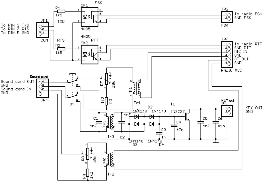
Fig. 1. The schematic
(click to enlarge)
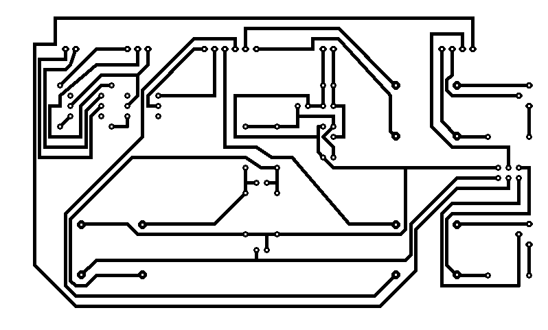
Fig. 2. The PC board pattern. Actual board size is 135 x 80 mm. This is a copper side view, good for PCB fabrication (use the enlarged version).
(click to enlarge)
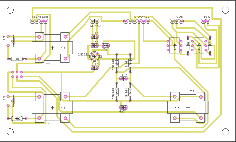
Fig. 3. The component layout (component side view).
(click to enlarge)
Troubleshooting
- The radio ground a the sound card ground (computer fround) must be kept away! The common trouble is lack of isolation (ground separation) resulting in audio hum, poor S/N ratio and unreliable port keying. Probably the best guide to overcome the ground isolation and common mode problems is the „RFI, Ferrites, and Common Mode Chokes For Hams“ by Jim Brown, K9YC (PDF download from http://www.audiosystemsgroup.com/RFI-Ham.pdf – a must have!). Don't forget the ferite chokes on all cables!
- Some optocouplers can't key the radio inputs, also some radios are known to have such problems. It is not a matter of the optocoupler gain but its output device (a transistor or a Darlington). Any optocoupler in its ON state represents a resistance in order of 3 – 15 ohms. Connect a 10 ohm resistor across the radio input (key, PTT, FSK) and watch the response. If the input is not keyed (or the output power is low), a solid state relay might help. The NAIS AQW210EH are good but rather expensive, but they are pin compatible with most optocouplers.
- Another source of problems can be the cable from computer port. The interface is universal but the cable not. Be careful of output signals where they are, on which pin! Most programs allowing to use RTS, DTR or BOTH for the PTT signal.
A PDF copy of this article is here.


Comments
Reaction
Submitted by Devon44986 (not verified) on
This is a good pcb design, how were you able to design this?
I like this website it’s a
Submitted by jackslesly19 (not verified) on
I like this website it’s a masterpiece! Glad I noticed this on google.
Cool
Submitted by Angel17 (not verified) on
Such an awesome post. Thanks for sharing this one. Drolet Myriad III
Informative!
Submitted by jacob96 (not verified) on
And also if I am not mistaken a sound card is an audio interface, right? residential spray foam service